|
CMOS Compatible Optical
Leaky Wave Antennas (OLWAs) and Devices Sponsored by NSF – ECCS |


|
|
|
MOTIVATION Ø What are Leaky Wave
Antennas? o Leaky wave antennas (LW
antennas) are travelling wave antennas that make use of the fast guided waves
to provide radiation. The LW radiates as it propagates through the waveguide o Fast-waves are also
named leaky waves, which mean the phase constant of the guided wave is
smaller than the free-space wave number. This type of waves ‘leak’ out of the
wave guide and can be utilized to design very directive antennas Ø Why “Optical”? o The optical frequency
range covers the electromagnetic spectrum extending from infrared (IR) to
ultraviolet (UV) o We are focusing on
radiation at 1550 nm, since it is the optical communication wavelength Ø Why SOI / CMOS
Compatibility? o It is basic chip
fabrication technology in use, accessible and cheap o It allows for reduced
parasitic capacitance and good mode confinement with low optical loss o It is compatible for
integration with CMOS electronics and can be tuned electronically to control far field
radiation |
|
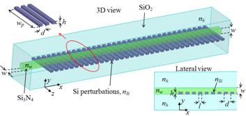
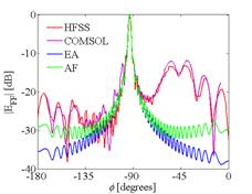
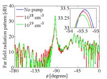
BASIC ANTENNA GEOMETRY AND RADIATION CAPABILITIES
Very directive radiation
is achieved. Beam width and beam angle are controlled by the LW phase
propagation and attenuation constants |
|||||||||
|
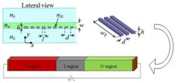
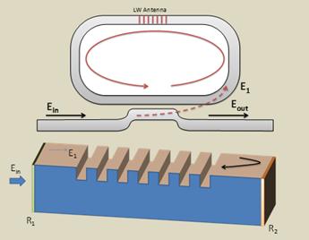
TWO DIFFERENT WAYS FOR
CONTROLLING THE RADIATION
Image taken from [4] This simple mechanism
currently does not provide great control of the radiated power at a single
direction. We are currently considering inserting the OLWA into resonators to
amplify the control |
|
ENHANCEMENT OF RADIATION
CONTROL BY INTEGRATING OLWA WITH A RESONATOR
Integrating OLWAs with
an optical resonator (ring or a linear cavity resonator) is one way of
achieving enhanced radiation control. In both cases, the variation of the
refractive index and losses will imply less coupling to the cavity and also a
weaker field in the cavity [5-7]. |
|
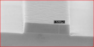
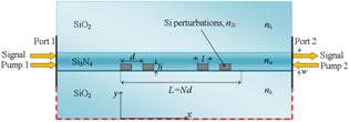
FABRICATION Fabrication of antennas
on silicon nitride on silicon: waveguides with strained dielectrics and
strained semiconductors has been fabricated. Currently nitride thickness is
being optimized for proposed antenna design.
Before we start
patterning with e-beam lithography, we developed the fabrication steps for strained
thick waveguide materials. In particular we use silicon on insulator, silicon
on sapphire and silicon nitride on silicon to control etch
profiles and waveguide smoothness for low loss operation. The difficulty of
the process arises due to strain level that leads to uneven etching and high
side wall roughness. Currently 4-step etching process has been adopted to
overcome this limitation. In the worst case scenario of highly strained
silicon on sapphire we achieve RMS surface roughness less than 25nm, Fig. 9.
In the following steps we optimize the growth of waveguide grade silicon
nitride on silicon to achieve 1μm thickness. |